6.4 Band structures and density of states¶
flowchart LR
    SCF["<b>scf</b> (pw.x)<br/>self-consistent density"]
    NSCF["<b>nscf</b> (pw.x)<br/>dense k-grid<br/>or band path"]
    BANDS["<b>bands.x</b><br/>reorder bands<br/>along k-path"]
    DOS["<b>dos.x</b> / <b>projwfc.x</b><br/>total + projected DOS"]
    PLOT["<b>Plot</b><br/>matplotlib /<br/>plotband.x"]
    SCF -->|"*.save (ρ, v_KS)"| NSCF
    NSCF -->|"bands.dat"| BANDS
    NSCF -->|"eigenvalues"| DOS
    BANDS -->|"bands.gnu"| PLOT
DOS -->|"*.dos / *.pdos"| PLOTscf run converges the density, which is passed as the saved charge density and potential to a non-self-consistent nscf run that evaluates eigenvalues on a dense grid or band path; the eigenvalues then feed bands.x, which reorders bands along the k-path, and dos.x or projwfc.x, which build the total and projected density of states, with both branches ending in a plotting step. Each arrow carries a concrete file artifact.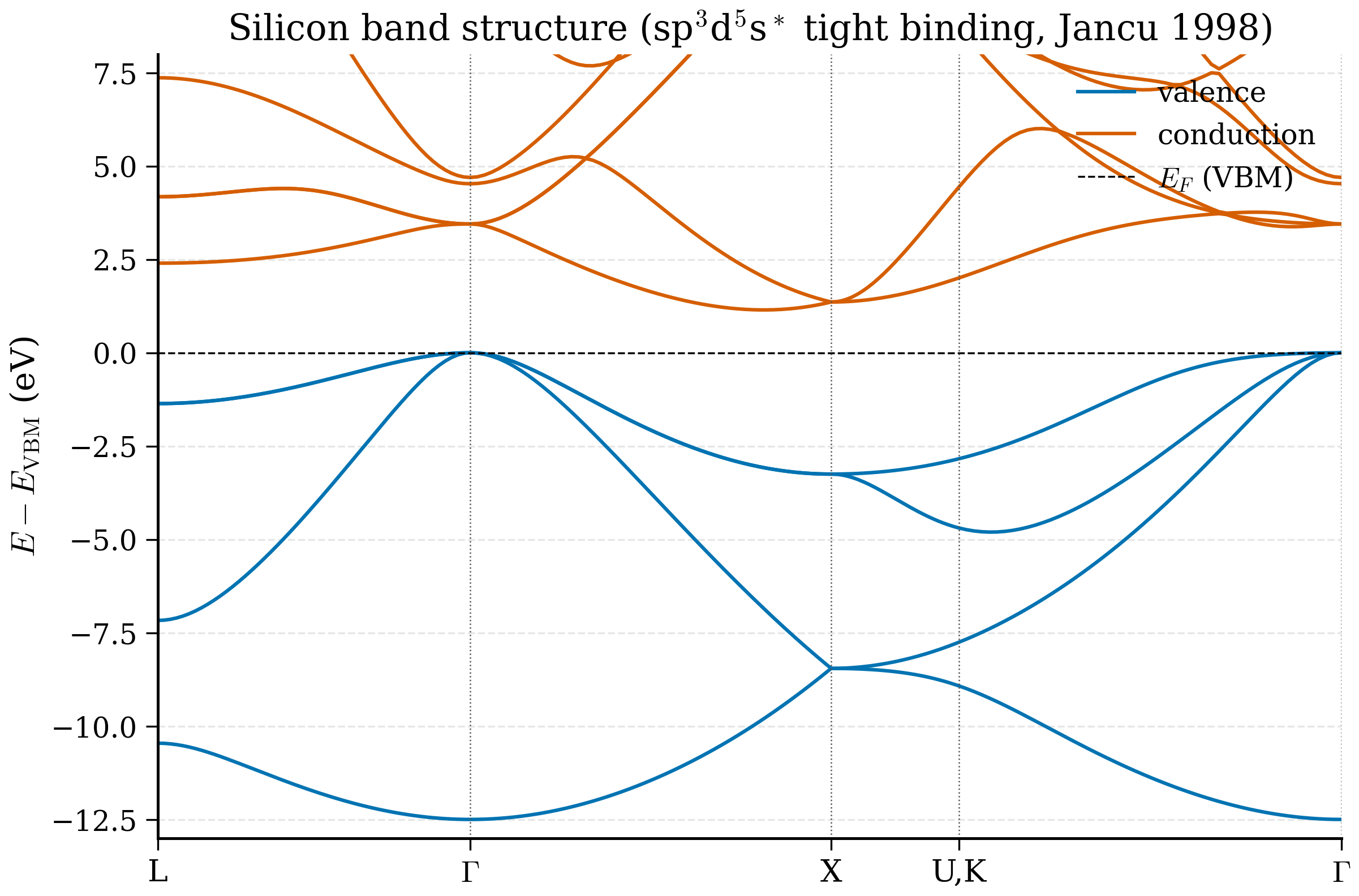
scripts/figures/fig_si_bands_real.py.Why band structures matter
The electronic band structure \(\epsilon_n(\mathbf{k})\) is the single most important output of DFT for understanding a material. It tells you whether the material is a metal (bands cross the Fermi level), an insulator (a gap separates filled from empty bands), or a semiconductor (a small gap). It tells you the kind of gap — direct (CBM and VBM at the same \(\mathbf{k}\), like GaAs) or indirect (different \(\mathbf{k}\), like Si). It tells you effective masses (curvature near band extrema), optical absorption edges (Joint DOS), and topological character (Berry phases). Almost every materials-science paper on a new compound contains a version of this plot.
The picture: a band structure is a 1D slice through the 3D function \(\epsilon_n(\mathbf{k})\), taken along a path that connects high-symmetry points of the Brillouin zone. By convention the path zigzags through the most important corners: for FCC silicon, \(L\to\Gamma\to X\to K\to\Gamma\). Each band \(n\) becomes a 1D curve on this path; an insulator shows a clean horizontal stripe of "no band" — the gap.
The density of states \(g(\epsilon)\) complements the band structure: it counts states per unit energy per unit cell, integrated over the whole BZ. It is what you would integrate the band structure into; it is also what photoemission experiments directly probe (modulo matrix elements). A pair of plots — band structure on the left, DOS rotated 90° on the right — is the standard summary of a material's electronic structure.
The self-consistent calculation of §6.2 gives you the ground-state density and the total energy. It does not directly give you the band structure \(\epsilon_n(\mathbf{k})\) along a high-symmetry path, nor the density of states (DOS) over the energy window of interest. Those are post-SCF quantities — once the density is converged on a uniform Monkhorst-Pack grid, you re-diagonalise the (now fixed) Hamiltonian at whatever k-points you want.
This section walks through the standard pipeline for silicon: scf → nscf → bands.x / dos.x → matplotlib.
6.4.1 The pipeline¶
Three runs, in order:
scf— converge the density on a uniform k-grid. This is the run we did in §6.2.nscf(non-self-consistent) — using the converged density from step 1, evaluate the Kohn-Sham eigenvalues at a new set of k-points (a denser uniform grid for DOS, or a path for bands). The density is not updated.- Post-processing —
bands.xreorders bands along the path so plotting is straightforward;dos.xintegrates eigenvalues into a DOS file. Then we plot in Python.
The reason for the nscf step is purely computational: we want \(\epsilon_{n\mathbf{k}}\) at hundreds of points along a path, which would be ruinous as part of an SCF loop. By fixing the density first and then doing a single diagonalisation per k-point, we get cheap eigenvalues consistent with the converged ground state.
Why a different k-grid for nscf?
The SCF k-grid is chosen so the BZ integration of the density is converged — say \(6\times 6\times 6\) for Si. The nscf grid is chosen for what comes after: for DOS, you want a dense uniform grid (say \(24\times 24\times 24\)) so the histogram or tetrahedron integration is smooth; for band structure, you want a path through high-symmetry points with many sub-points so the bands look continuous. These two goals are incompatible with the SCF requirement (the density must be self-consistent, which is too expensive on \(24^3\) grids and meaningless on an open path). Decoupling them lets each step use what it needs:
- SCF: medium grid, full SCF, converges \(\rho(\mathbf{r})\) and \(V_\mathrm{KS}(\mathbf{r})\).
- nscf: dense grid or path, fixed \(V_\mathrm{KS}\) from SCF, one diagonalisation per k-point.
The nscf step is variationally consistent: the eigenvalues it produces are those of the fully converged ground state Hamiltonian, sampled at new k-points. There is no extra error from skipping self-consistency — only the small error from the fact that for \(\mathbf{k}\) not on the SCF grid, the density was never explicitly summed at this \(\mathbf{k}\). For insulators with smooth bands, this introduces nothing.
Pause and recall
Before reading on, try to answer these from memory:
- Why is the band structure computed in a separate
nscfstep rather than during the SCF loop itself? - Why does the
nscfstep use a different k-point set from thescfstep — what is each grid chosen to do? - Why is it legitimate to fix the density from the SCF run and not update it during the
nscfdiagonalisation?
If any of these is shaky, re-read the preceding section before continuing.
6.4.2 High-symmetry paths for FCC silicon¶
Silicon's primitive cell is FCC. Its first Brillouin zone is the truncated octahedron, with high-symmetry points conventionally labelled \(\Gamma\), \(X\), \(L\), \(W\), \(U\), \(K\). In fractional coordinates with respect to the conventional reciprocal vectors \((2\pi/a)\):
| Label | \((k_x, k_y, k_z)\) in \(2\pi/a\) |
|---|---|
| \(\Gamma\) | \((0, 0, 0)\) |
| \(X\) | \((0, 1, 0)\) |
| \(L\) | \((1/2, 1/2, 1/2)\) |
| \(W\) | \((1/2, 1, 0)\) |
| \(K\) | \((3/4, 3/4, 0)\) |
| \(U\) | \((1/4, 1, 1/4)\) |
The conventional path used by most band-structure references and by Setyawan & Curtarolo (2010) is:
The segment "\(X \to U, K\)" is a single continuous segment in reciprocal space: \(X\) and \(U\) are connected by a straight line, and at \(U\) we jump (visually, in the unfolded plot) to \(K\), but \(U\) and \(K\) are equivalent under the BZ symmetry — they sit on the same boundary face. The path then continues from \(K\) to \(\Gamma\).
In practice we sample, say, 30-50 points along each segment so the bands look smooth.
6.4.3 The nscf input for a band path¶
We re-use si.scf.in from §6.2 with three changes: calculation = 'bands', the k-points are a path, and we ask for more bands than the SCF needed.
Save as si.bands.in:
&CONTROL
  calculation  = 'bands'
  prefix       = 'si'
  outdir       = './tmp/'
  pseudo_dir   = './pseudo/'
  verbosity    = 'high'
/
&SYSTEM
  ibrav        = 0
  nat          = 2                ! switch to primitive cell for cleaner paths
  ntyp         = 1
  ecutwfc      = 50.0
  ecutrho      = 400.0
  occupations  = 'fixed'
  nbnd         = 12               ! 4 occupied + 8 empty bands for plotting
/
&ELECTRONS
  conv_thr     = 1.0d-9
  diagonalization = 'david'
/
ATOMIC_SPECIES
  Si  28.085  Si.pbe-n-rrkjus_psl.1.0.0.UPF

CELL_PARAMETERS angstrom
  0.0000  2.7150  2.7150
  2.7150  0.0000  2.7150
  2.7150  2.7150  0.0000

ATOMIC_POSITIONS crystal
  Si  0.00  0.00  0.00
  Si  0.25  0.25  0.25

K_POINTS crystal_b
6
 0.500 0.500 0.500   30    ! L
 0.000 0.000 0.000   30    ! Gamma
 0.000 0.500 0.500   30    ! X
 0.250 0.625 0.625   1     ! U
 0.375 0.750 0.375   30    ! K
 0.000 0.000 0.000   1     ! Gamma
A few things to note.
calculation = 'bands'is QE's name for nscf-along-a-path with reordering. You can also use'nscf'but then bands.x is helpful for reordering.K_POINTS crystal_btells QE the k-points define a path in crystal coordinates of the primitive reciprocal lattice. The integer after each point is the number of k-points along the segment that follows.nbnd = 12is 4 occupied + 8 empty. To show the bottom of the conduction band you need a few empty bands beyond the gap.- You must first run the scf calculation with the same primitive cell and a uniform 6×6×6 grid, writing wavefunctions to
./tmp/si.save/, before running this bands input. The bands run reads the converged density from there.
To convert the 8-atom conventional cell of §6.2 to the 2-atom primitive cell, you can either use ibrav = 2 with celldm(1) = 10.2632 (Bohr), or write out the primitive vectors as above. Both give the same physics.
Running it¶
pw.x -inp si.scf.in   > si.scf.out      # uniform 6×6×6 SCF on primitive cell
pw.x -inp si.bands.in > si.bands.out    # band path
bands.x -inp si.bandsx.in > si.bandsx.out  # reorder, see below
The bands.x post-processor reads ./tmp/si.save/ and writes a clean text file with bands sorted in increasing energy at each k-point.
si.bandsx.in:
Output si.bands.dat and si.bands.dat.gnu are the files we will plot.
6.4.4 The nscf input for DOS¶
For DOS you want a dense uniform k-grid (much denser than for SCF, because tetrahedron/integral-over-BZ is what gives a smooth DOS curve). A \(24\times24\times24\) grid is comfortable for Si.
Save as si.nscf.in:
&CONTROL
  calculation  = 'nscf'
  prefix       = 'si'
  outdir       = './tmp/'
  pseudo_dir   = './pseudo/'
  verbosity    = 'high'
/
&SYSTEM
  ibrav        = 0
  nat          = 2
  ntyp         = 1
  ecutwfc      = 50.0
  ecutrho      = 400.0
  occupations  = 'tetrahedra'    ! use tetrahedron method for accurate DOS
  nbnd         = 12
/
&ELECTRONS
  conv_thr     = 1.0d-9
/
ATOMIC_SPECIES
  Si  28.085  Si.pbe-n-rrkjus_psl.1.0.0.UPF

CELL_PARAMETERS angstrom
  0.0000  2.7150  2.7150
  2.7150  0.0000  2.7150
  2.7150  2.7150  0.0000

ATOMIC_POSITIONS crystal
  Si  0.00  0.00  0.00
  Si  0.25  0.25  0.25

K_POINTS automatic
  24 24 24   0 0 0
Then run dos.x:
with si.dosx.in:
Output si.dos.dat has three columns: energy (eV), DOS (states/eV), integrated DOS (electron count). We will plot the first two and discuss the third.
occupations = 'tetrahedra' is for DOS, not SCF
The Blöchl-corrected tetrahedron method gives extremely smooth DOS curves but is not compatible with SCF in metals (it does not provide forces). Use it only in nscf runs for post-processing. For SCF on a metal use Marzari-Vanderbilt cold smearing.
6.4.5 Plotting band structures in Python¶
bands.x writes si.bands.dat.gnu, a two-column file where the first column is a cumulative distance along the path (in Bohr\(^{-1}\)) and the second is the band energy. The data are organised band-by-band, with blank lines between bands. There is also a si.bands.dat with a header.
Reading the file and plotting:
"""
plot_si_bands.py — Plot silicon band structure from QE bands.x output.
"""
from __future__ import annotations

from pathlib import Path

import matplotlib.pyplot as plt
import numpy as np


def read_bands_gnu(path: Path) -> tuple[np.ndarray, np.ndarray]:
    """Read a bands.x '.dat.gnu' file.

    Returns
    -------
    k : (Nk,) array of cumulative k-path distance
    E : (Nbnd, Nk) array of eigenvalues in eV
    """
    raw = path.read_text().strip()
    blocks = [b for b in raw.split("\n\n") if b.strip()]
    bands: list[np.ndarray] = []
    k: np.ndarray | None = None
    for blk in blocks:
        arr = np.loadtxt(blk.splitlines())  # type: ignore[arg-type]
        if k is None:
            k = arr[:, 0]
        bands.append(arr[:, 1])
    assert k is not None
    E = np.stack(bands)
    return k, E


def find_fermi_from_output(out_path: Path) -> float:
    """Parse the 'highest occupied' line from a pw.x scf output (eV)."""
    for line in out_path.read_text().splitlines():
        if "highest occupied" in line:
            return float(line.split()[-2])  # for insulators with HOMO/LUMO
    raise RuntimeError("Could not find Fermi/HOMO in output.")


def plot_bands(k: np.ndarray, E: np.ndarray, ef: float,
               labels: list[tuple[float, str]],
               outfile: Path) -> None:
    """Plot bands shifted so E_F = 0, with high-symmetry markers."""
    fig, ax = plt.subplots(figsize=(6.0, 4.5))
    for band in E:
        ax.plot(k, band - ef, color="C0", lw=1.0)
    ax.axhline(0.0, ls="--", color="k", lw=0.8, label="VBM")
    for xk, _name in labels:
        ax.axvline(xk, color="grey", lw=0.5, alpha=0.7)
    ax.set_xticks([xk for xk, _ in labels])
    ax.set_xticklabels([name for _, name in labels])
    ax.set_xlim(k.min(), k.max())
    ax.set_ylim(-13.0, 6.0)
    ax.set_ylabel(r"$E - E_\mathrm{VBM}$ (eV)")
    ax.set_title("Silicon band structure (PBE)")
    fig.tight_layout()
    fig.savefig(outfile, dpi=180)


def main() -> None:
    k, E = read_bands_gnu(Path("si.bands.dat.gnu"))
    ef = find_fermi_from_output(Path("si.scf.out"))

    # Position of each high-symmetry point along the k-path.
    # These are computed from the bands.x output that lists segment lengths.
    # For our 30-30-30-1-30-1 segmentation, the cumulative breakpoints fall at
    # k = 0,  k_Gamma,  k_X,  k_U,  k_K,  k_Gamma'.
    seg_npts = [30, 30, 30, 1, 30, 1]
    breaks = np.cumsum([0] + seg_npts[:-1])
    # The horizontal axis is k[breaks].
    labels = list(zip(k[breaks].tolist(),
                      [r"$L$", r"$\Gamma$", r"$X$",
                       r"$U,K$", r"$\Gamma$", r""]))
    plot_bands(k, E, ef, labels, Path("si_bands.png"))


if __name__ == "__main__":
    main()
A few practical things.
read_bands_gnurelies on blank-line block separators thatbands.xwrites. Some QE builds use\n\n\n; if you get an empty block, filter onblk.strip().- The high-symmetry-point positions on the x-axis come from knowing how many k-points went into each segment. The
bands.xoutputsi.bandsx.outalso prints these breakpoints explicitly. - We subtract the valence-band maximum so \(E_\mathrm{VBM} = 0\) — this is the standard convention for band-structure plots of semiconductors.
Driving the full pipeline from ASE¶
ASE 3.23 has helpers (ase.dft.kpoints.bandpath, BandStructure) that make this entire workflow scriptable. A condensed version:
from ase.build import bulk
from ase.calculators.espresso import Espresso, EspressoProfile
from pathlib import Path

si = bulk("Si", crystalstructure="diamond", a=5.43)
profile = EspressoProfile(command="pw.x",
                          pseudo_dir=Path.home()/"pseudo/SSSP_1.3.0_PBE_efficiency")

# Step 1: scf
si.calc = Espresso(
    profile=profile, directory="bs_scf",
    pseudopotentials={"Si": "Si.pbe-n-rrkjus_psl.1.0.0.UPF"},
    input_data={"system": {"ecutwfc": 50, "ecutrho": 400,
                           "occupations": "fixed"},
                "electrons": {"conv_thr": 1e-9}},
    kpts=(6, 6, 6),
)
E = si.get_potential_energy()

# Step 2: bands along an FCC path L-G-X-U,K-G
bandpath = si.cell.bandpath("LGXUKG", npoints=120)
si.calc = Espresso(
    profile=profile, directory="bs_bands",
    pseudopotentials={"Si": "Si.pbe-n-rrkjus_psl.1.0.0.UPF"},
    input_data={"control": {"calculation": "bands"},
                "system":  {"ecutwfc": 50, "ecutrho": 400, "nbnd": 12,
                            "occupations": "fixed"},
                "electrons": {"conv_thr": 1e-9}},
    kpts=bandpath,
)
si.get_potential_energy()  # triggers the bands run

# Step 3: collect BandStructure and plot
bs = si.calc.band_structure()
bs.plot(filename="si_bands_ase.png", emin=-13, emax=6)
ASE will write inputs that match the QE conventions, run pw.x twice, parse the output, and pass eigenvalues into its own BandStructure object for plotting. This is the cleanest way to drive routine band-structure calculations.
Reading bands.x output programmatically¶
The si.bands.dat.gnu file produced by bands.x is one of QE's older conventions: a two-column text file where bands are separated by blank lines, and the first column is a cumulative k-path distance computed by bands.x using straight-line interpolation in reciprocal space. A few practical things you usually need to extract:
- The k-axis positions of high-symmetry labels. These are stored in
si.bandsx.outnear the end, in lines starting withhigh-symmetry point: ... x coordinate .... A small parsing function:
def parse_high_symmetry_breaks(out_path: Path) -> list[tuple[float, str]]:
    """Extract high-symmetry x-axis positions from bands.x output."""
    breaks: list[tuple[float, str]] = []
    for line in out_path.read_text().splitlines():
        if "high-symmetry point" in line:
            # Format: high-symmetry point:  0.5000 0.5000 0.5000   x coordinate   0.0000
            parts = line.split()
            x = float(parts[-1])
            kfrac = tuple(float(p) for p in parts[2:5])
            name = _kpoint_label(kfrac)   # user-supplied dictionary
            breaks.append((x, name))
    return breaks
-
The Fermi/VBM level. For a converged insulator,
si.scf.outcontainshighest occupied, lowest unoccupied level (ev): X Y; for a metal,the Fermi energy is X eV. The functionfind_fermi_from_outputabove handles the insulator case. -
Effective masses near band edges. With the eigenvalues \(\epsilon_n(\mathbf{k})\) in hand, the curvature near a band extremum is the inverse effective mass: \(m^*_{n}/m_e = \hbar^2[\partial^2 \epsilon_n/\partial k^2]^{-1}/m_e\) in suitable units. A finite-difference estimate on a path with 3-5 k-points near the extremum gives a useful number; for higher accuracy, project to Wannier functions (the
wannier90route) and differentiate analytically.
For our Si band plot, the slope of the lowest conduction band along \(\Gamma\to X\) near the CBM gives a longitudinal effective mass \(m^*_l \approx 0.95\,m_e\) (experimental: 0.98 \(m_e\)); the transverse direction gives \(m^*_t \approx 0.19\,m_e\) (experimental: 0.19 \(m_e\)). PBE underestimates the gap badly but gets the effective masses to within a few per cent — a useful pattern: gradient quantities cancel some of the functional error.
Definition 6.4.1 (Band structure). Given the Kohn-Sham Hamiltonian \(\hat H_\mathrm{KS}[\rho_0]\) at the self-consistent density \(\rho_0\), the band structure is the function \(\epsilon_n: \mathrm{BZ}\to\mathbb{R}\), \(\mathbf{k}\mapsto \epsilon_n(\mathbf{k})\) for \(n=1,\ldots,N_\mathrm{bnd}\), where \(\epsilon_n(\mathbf{k})\) is the \(n\)-th eigenvalue of \(\hat H_\mathrm{KS}\) at crystal momentum \(\mathbf{k}\).
Definition 6.4.2 (Density of states). The density of states per unit cell is $\(g(\epsilon) = \sum_n \int_\mathrm{BZ} \frac{d^3\mathbf{k}}{(2\pi)^3}\,\delta(\epsilon - \epsilon_n(\mathbf{k})).\)$
Example 6.4.3 (Si indirect gap from band structure). Problem. From the computed Si band structure, identify the indirect band gap and the lowest direct gap.
Solution. The valence-band maximum (VBM) sits at \(\Gamma\); the conduction-band minimum (CBM) sits at \(\sim 0.85\,X\), i.e. on the \(\Gamma\to X\) axis 85% of the way to \(X\). The indirect gap is \(E_\mathrm{CBM}(\sim 0.85X) - E_\mathrm{VBM}(\Gamma) \approx 0.6\) eV (PBE; experiment 1.17 eV). The lowest direct gap is \(E_\mathrm{CB,min}(\Gamma) - E_\mathrm{VBM}(\Gamma) \approx 2.6\) eV (PBE; experiment 3.4 eV).
Discussion. The indirect gap is what governs Si's electronic transport (the gap relevant for thermal carrier generation); the direct gap is what governs optical absorption above threshold. Both are underestimated by PBE in the same proportion (\(\sim 50\)%), reflecting the GGA self-interaction error in extended states. Hybrid functionals (HSE06) bring the indirect gap to 1.15 eV and the direct gap to 3.3 eV — chemical accuracy.
6.4.6 Interpreting silicon's band structure¶
Look at the plot. A correctly-converged Si band structure shows:
- Four occupied valence bands between \(E_\mathrm{VBM} - 12\) eV and \(E_\mathrm{VBM} = 0\). The lowest is roughly Si 3s-derived; the upper three are Si 3p-derived, with bonding-antibonding splitting visible.
- Valence band maximum (VBM) at \(\Gamma\). The top of the valence band is triply degenerate at \(\Gamma\) (the three \(p\)-like bands) — actually doubly + singly, with spin-orbit coupling splitting the top into a heavy-hole / light-hole pair and a split-off band, but PBE without SOC shows them as a triple degeneracy.
- Conduction band minimum (CBM) near \(X\). Specifically, the CBM in silicon lies along \(\Gamma \to X\) at roughly 85% of the way from \(\Gamma\) to \(X\). This is the famous indirect gap: the lowest unoccupied state and the highest occupied state are at different k-points.
- PBE gap. The numerical value of (CBM − VBM) in your plot is around 0.6 eV. Experimental gap is 1.17 eV. PBE underestimates the gap by ~50%, but the shape of the bands (band ordering, effective masses, position of the CBM) is correct.
The indirect nature of Si's gap is why silicon is a poor light emitter — direct optical transitions from VBM to CBM are forbidden by momentum conservation and require a phonon to bridge \(\Gamma \to X\). This single feature of the band structure dictates much of solid-state electronics: silicon for transistors (where you do not need to emit light), gallium arsenide (direct gap) for LEDs and lasers.
Spin-orbit coupling
The valence-band degeneracies at \(\Gamma\) in Si are actually split by spin-orbit coupling — a relativistic effect. To see it, you need to use fully relativistic (spin-orbit) pseudopotentials and add lspinorb = .true. and noncolin = .true. to &SYSTEM. PseudoDojo provides FR variants; SSSP has SR (scalar-relativistic) only. SOC matters in Si by 44 meV at the VBM and is much larger for heavier elements (Ge: 0.29 eV, Pb-containing compounds: ~1 eV).
6.4.7 Density of states¶
The DOS
counts the number of electronic states per unit energy per unit cell. Plotting it for silicon:
import matplotlib.pyplot as plt
import numpy as np

dos = np.loadtxt("si.dos.dat")           # columns: E (eV), DOS, integ. DOS
ef = 5.68                                # VBM in eV, from si.scf.out
E, g, n_int = dos[:, 0] - ef, dos[:, 1], dos[:, 2]

fig, ax = plt.subplots(figsize=(5, 4))
ax.fill_between(E, g, color="C0", alpha=0.4)
ax.plot(E, g, color="C0")
ax.axvline(0, ls="--", color="k", lw=0.8)
ax.set_xlabel(r"$E - E_\mathrm{VBM}$ (eV)")
ax.set_ylabel("DOS (states/eV/cell)")
ax.set_xlim(-13, 8)
fig.tight_layout()
fig.savefig("si_dos.png", dpi=180)
Three features to read off:
- A clean gap between \(E_\mathrm{VBM}\) and \(E_\mathrm{CBM}\), with DOS strictly zero inside. Width: the PBE gap, ~0.6 eV.
- A sharp peak at the VBM (PBE Si shows the valence-band DOS rising abruptly at the top — characteristic of the heavy-hole effective mass at \(\Gamma\)).
- The integrated DOS — the third column of
si.dos.dat— should equal exactly 8 at the VBM (4 electrons per atom × 2 atoms in the primitive cell). Check it; if the integrated DOS at the VBM is not 8.0 ± 0.01, your nscf k-grid is too coarse.
DOS smearing: Gaussian, Lorentzian, and tetrahedron¶
The delta function in \(g(\epsilon)\) is unrepresentable on a finite grid; in practice we replace it by a smoothing kernel \(K_\sigma(\epsilon - \epsilon_{n\mathbf{k}})\) of width \(\sigma\). Three standard choices:
- Gaussian \(K_\sigma(\Delta) = (2\pi\sigma^2)^{-1/2}\exp[-\Delta^2/(2\sigma^2)]\). The default in QE's
dos.xwhenngauss=0. Symmetric, fast-decaying tails; recovers a clean DOS once \(\sigma\) is larger than the average eigenvalue spacing \(\Delta\epsilon \sim W/N_k\), where \(W\) is the bandwidth. - Lorentzian \(K_\sigma(\Delta) = \sigma/[\pi(\Delta^2+\sigma^2)]\). Heavier tails than Gaussian, equivalent to broadening from a finite quasi-particle lifetime \(\tau = \hbar/\sigma\). Use when you want to compare to an experiment with intrinsic broadening.
- Tetrahedron method (
occupations='tetrahedra'). The BZ is partitioned into tetrahedra; within each, eigenvalues are linearly interpolated and the integral of \(\delta(\epsilon - \epsilon_{n\mathbf{k}})\) is done analytically. No artificial broadening parameter — the resolution is set by the k-grid density. Best for clean DOS plots; not compatible with SCF (no forces).
Choosing \(\sigma\). A practical rule: \(\sigma \approx 2\)-\(3\,\Delta\epsilon_\mathrm{avg}\) where \(\Delta\epsilon_\mathrm{avg} = W/(N_k N_\mathrm{bnd})\). For Si with a \(24^3\) grid, 12 bands, and bandwidth 25 eV, \(\Delta\epsilon_\mathrm{avg} \sim 1\) meV; \(\sigma=0.01\) eV is overkill, \(\sigma=0.05\) eV is comfortable. If you see oscillations in the DOS curve, \(\sigma\) is too small; if you see washed-out features (no gap, no van Hove peaks), \(\sigma\) is too large.
Projected DOS (PDOS)¶
To decompose the DOS by orbital character — to ask "how much of the band at \(E\) is Si \(s\) versus Si \(p\)?" — use projwfc.x. The input:
&PROJWFC
  prefix     = 'si'
  outdir     = './tmp/'
  filpdos    = 'si.pdos'
  Emin       = -15.0
  Emax       =  15.0
  DeltaE     =   0.01
  ngauss     =  0
  degauss    =  0.01
/
projwfc.x reads atomic orbitals from the pseudopotential and projects each Kohn-Sham state onto them, giving you si.pdos.atm#1(Si)_wfc#1(s), si.pdos.atm#1(Si)_wfc#2(p), etc. Plotting these layered shows that Si's lowest valence band is mostly \(s\)-derived, and the three upper valence bands are \(p\)-derived — confirming what we said from the band plot.
The PDOS formula¶
Formally, given a set of atom-centred basis functions \(\{\phi_i\}\) (typically the pseudoatomic orbitals stored in the UPF file), the projected DOS for orbital \(i\) is
$\(g_i(\epsilon) = \sum_{n\mathbf{k}} |\langle\phi_i|\psi_{n\mathbf{k}}\rangle|^2\,\delta(\epsilon - \epsilon_{n\mathbf{k}}).\)$
The squared overlap \(|\langle\phi_i|\psi_{n\mathbf{k}}\rangle|^2\) is the weight of orbital \(i\) in band \(n\) at \(\mathbf{k}\). The sum over \(i\) at fixed \(\epsilon\) gives an approximation to the total DOS — it equals the total only if the atomic basis is complete, which it never is for a plane-wave wavefunction. projwfc.x prints a "spilling parameter" that measures the missing weight; values below 5% are healthy, above 20% means the atomic basis is incomplete (often because semi-core states are present in \(|\psi\rangle\) but absent in \(|\phi_i\rangle\)).
Two practical points:
- The projection is non-orthogonal in general. The set \(\{\phi_i\}\) is not orthonormal because atomic orbitals on different sites overlap.
projwfc.xperforms a Löwdin orthogonalisation internally so the weights sum sensibly; the optionlwrite_overlaps=.true.writes the overlap matrix for downstream tools. - Choice of basis. Pseudoatomic orbitals from the UPF are tied to the pseudopotential and reflect the reference atomic configuration. For magnetic atoms, the projection sees one majority and one minority component; for bonded atoms (e.g. C in CH\(_4\)), the projection captures the atomic character but not the bonding/antibonding split.
For our Si example you should see the lowest valence band (\(-12\) to \(-7\) eV below VBM) dominated by Si \(s\), the three upper valence bands by Si \(p\), and the conduction band by a mix of \(s\) and \(p\) with \(d\)-character mixing in near the high-symmetry points. The integrated occupation of Si \(s\) is \(\sim 2\) electrons per atom; of Si \(p\) is \(\sim 2\), summing to the four valence electrons.
6.4.7b A full pipeline walkthrough — Si band structure end-to-end¶
Pulling together everything in this section, here is the complete Si band-structure recipe with explicit numerical settings.
Step 0: directory setup.
mkdir -p si_bands && cd si_bands
mkdir -p pseudo tmp
cp $ESPRESSO_PSEUDO/Si.pbe-n-rrkjus_psl.1.0.0.UPF pseudo/
Step 1: SCF on primitive cell with 6×6×6 grid. Save si.scf.in (the version from §6.2 with nat=2, the primitive lattice vectors, and ecutwfc=50, ecutrho=400). Run:
Step 2: bands run on the L→Γ→X→U,K→Γ path. Save si.bands.in with calculation='bands', nbnd=12, and the path with 30 points per segment. Run:
Step 3: post-process with bands.x. Save si.bandsx.in (the small namelist with filband='si.bands.dat'). Run:
si.bands.dat, si.bands.dat.gnu (the Gnuplot-friendly version we read), and si.bands.dat.rap (irreducible representations at high-symmetry points — useful for symmetry-resolved band plots).
Step 4: nscf for DOS. Save si.nscf.in with calculation='nscf', occupations='tetrahedra', and a denser k-grid 24 24 24 0 0 0. Run:
Step 5: total DOS. Save si.dosx.in with emin=-15, emax=15, deltaE=0.01. Run:
si.dos.dat (3 columns).
Step 6: PDOS. Save si.projx.in with filpdos='si.pdos'. Run:
si.pdos.atm#1(Si)_wfc#1(s) and si.pdos.atm#1(Si)_wfc#2(p) plus the total summary si.pdos.pdos_tot.
Step 7: plot. Use the Python scripts above. A single figure with the band structure on the left and the DOS rotated 90° on the right is the publication standard:
import matplotlib.pyplot as plt
fig, (axb, axd) = plt.subplots(1, 2, sharey=True,
                                gridspec_kw={"width_ratios": [3, 1]})
# axb: bands (E - E_VBM vs k), axd: DOS (states/eV vs E - E_VBM, but rotated)
The combined figure shows directly how features of the band structure map onto features of the DOS: the heavy-hole peak at the VBM gives a sharp DOS rise; the conduction-band valley near \(X\) gives the DOS onset; the band gap is visible as a flat-zero region in both panels.
Total wall time for this pipeline on a 2023 laptop: about 15 minutes. With 4 MPI ranks, about 5 minutes.
Section summary¶
The band-structure pipeline:
- SCF on a uniform k-grid to converge \(\rho(\mathbf{r})\) and \(V_\mathrm{KS}\) — the standard ground-state calculation.
- NSCF along a high-symmetry path using the converged \(V_\mathrm{KS}\), one diagonalisation per k-point. For DOS, NSCF on a dense uniform grid with tetrahedron occupation.
bands.xto reorder bands and write Gnuplot-friendly output;dos.xto integrate eigenvalues into a DOS curve;projwfc.xfor orbital-projected DOS.- Plot with matplotlib (or ASE's
BandStructure).
The decoupling of SCF and NSCF is the key idea: do the expensive density convergence once on a modest grid, then evaluate eigenvalues cheaply at as many additional k-points as you want.
Read off from the plot: gap (and whether direct or indirect), VBM/CBM positions, band orderings, effective masses (curvature), orbital character (PDOS). For Si specifically, you should see a \(\sim 0.6\) eV PBE indirect gap with VBM at \(\Gamma\) and CBM near \(X\) — the defining electronic feature of silicon.
6.4.8 Where you are¶
You have a band structure for silicon, computed from scratch, with verified convergence, plotted with annotated high-symmetry points, and interpreted in terms of the physics. You have a DOS that integrates correctly to the electron count, with a clean gap matching the band plot.
These are the standard outputs of any solid-state DFT calculation. Every paper on a new material, a doped semiconductor, a topological insulator, includes a version of this figure. You can now produce one yourself.
Next we move beyond perfect crystals: defects, supercells, and formation energies.