3b.2 — The Nearly Free Electron Model¶
"Most metals look free-electron until you measure them carefully." — folklore
Why does the nearly-free-electron model exist?
The puzzle: Free electrons in a metal — by the Drude model and the Sommerfeld treatment of the next section — explain a lot: electrical conductivity, the linear-in-\(T\) specific heat, the Wiedemann-Franz law. But they predict that every solid should be a metal. Experimentally, of course, most materials are not metals; they are insulators or semiconductors with a gap between filled and empty states. Where does the gap come from?
The Bragg analogy: in 1928 the answer was discovered by analogy with X-ray diffraction. When an X-ray with wavevector \(\mathbf k\) such that \(|\mathbf k|^2 = |\mathbf k+\mathbf G|^2\) hits a crystal, it scatters strongly off the lattice — this is Bragg reflection. The same condition for electron wavefunctions creates a standing wave that does not propagate. The electron with wavevector \(\mathbf k\) satisfying the Bragg condition cannot exist as a freely propagating state; it sits as a standing wave with one of two possible energies, depending on whether its probability density sits on or between the ions. Those two energies differ by twice the Fourier coefficient of the lattice potential — and that is the band gap.
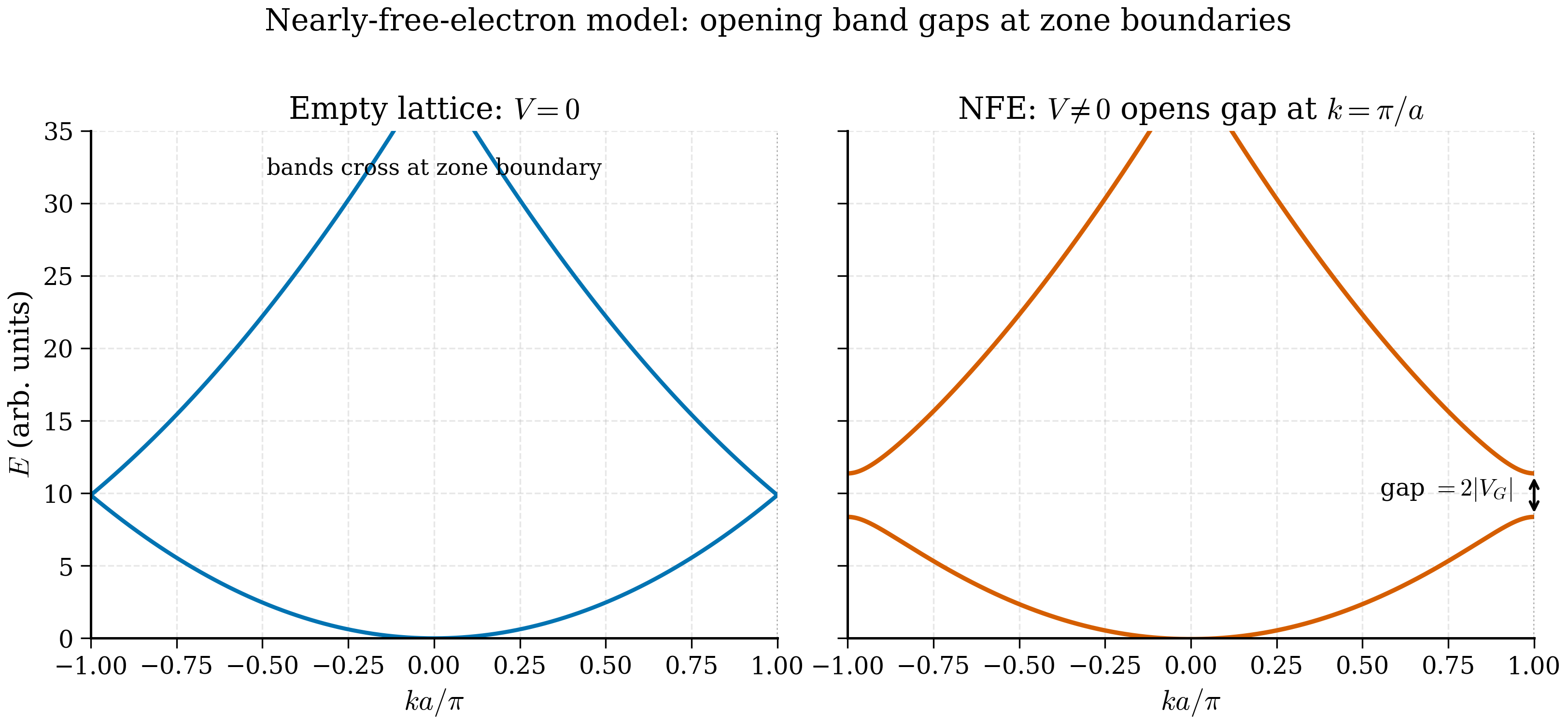
The picture to keep: start with free electron parabolas \(E = \hbar^2 k^2/2m\). Fold them back into the first BZ. They cross at the BZ boundary. Turn on a tiny lattice potential — those crossings split into avoided crossings, with a gap of size \(2|V_\mathbf G|\). Every band gap in every material, no matter how small or large, is fundamentally this avoided crossing. The picture is so general that it survives even in DFT calculations where the "lattice potential" is replaced by the self-consistent Kohn–Sham potential.
What it buys us: an intuitive, calculable explanation of band gaps. The 30–100% gap underestimate of LDA/GGA, the success of hybrid functionals at fixing them, the structural origin of metallic vs insulating behaviour — all are visible in the NFE picture.
The previous section gave the structure of crystal eigenstates: \(\psi_{n\mathbf k}(\mathbf r) = e^{i\mathbf k\cdot\mathbf r}u_{n\mathbf k}(\mathbf r)\). It did not, however, tell us anything about the energies \(E_{n\mathbf k}\). To get those, you need a model. The two simplest models — and the two limits that bracket every real material — are the nearly free electron model (this section) and the tight-binding model (next section). They start from opposite ends and meet in the middle.
The nearly free electron (NFE) model is the appropriate starting point for metals such as Na, Al, Cu, and (with caveats) Si, where the valence electrons are spread out and the ionic pseudopotential is weak. We will see that even a weak periodic potential changes the qualitative picture in one essential way: it opens band gaps at the Brillouin-zone boundaries. The size of those gaps is the principal quantitative output of the model, and the mechanism by which they open is so general that it underlies every avoided crossing in solid state physics.
Intuition: a gentle bump in a sea of plane waves
Think of the conduction electrons in sodium or aluminium as a sea of nearly-free particles, slightly perturbed by the periodic dimples of the ionic cores. If the dimples were entirely absent (the empty-lattice limit), the eigenstates would be plain plane waves and the energy would be a single parabola \(\hbar^2 q^2/2m\), with no gaps. Now switch the dimples on. They are small in two senses: (i) the Fourier components \(V_\mathbf G\) of the periodic potential are small compared to the kinetic energy of an electron with wavelength \(\sim 1/|\mathbf G|\); (ii) the lattice introduces a new length scale \(a\), hence a new energy scale \(\hbar^2 (\pi/a)^2 / 2m\) — the kinetic energy of an electron with wavelength comparable to the lattice spacing.
Anywhere except at a Brillouin-zone boundary, the small dimples cause only small perturbative shifts of the free-electron parabolas. At the zone boundary, however, two plane waves with equal kinetic energy — one moving right, one moving left — are exactly degenerate, and the smallest perturbation can mix them strongly. The mixing creates two standing waves whose energies differ by an amount proportional to \(|V_\mathbf G|\). This is the band gap. The picture is so general that whenever a small perturbation acts on two exactly degenerate states, you should expect a \(|V|\)-sized splitting — the technical name is avoided crossing, and band gaps are its most famous example.
3b.2.1 The empty-lattice limit¶
Set \(V(\mathbf r) = 0\) in the single-particle Schrödinger equation. The eigenstates are plane waves \(e^{i\mathbf q\cdot\mathbf r}\) with continuous energy \(\hbar^2 q^2/2m\). As we noted at the end of §3b.1, we can repackage them in Bloch form by writing \(\mathbf q = \mathbf k + \mathbf G\) with \(\mathbf k\) in the first Brillouin zone:
Each reciprocal lattice vector \(\mathbf G_n\) defines a "band" — a paraboloid in \(\mathbf k\)-space, shifted so that its minimum is at \(-\mathbf G_n\). When we restrict \(\mathbf k\) to the BZ, these paraboloids fold inward. The result is the empty-lattice band structure. For a 1D chain with lattice constant \(a\) the reciprocal lattice vectors are \(G_n = 2\pi n/a\) for \(n\in\mathbb Z\), and the BZ is \(-\pi/a \le k \le \pi/a\). The first few bands are
At the zone boundary \(k = \pi/a\), the bands \(E_0^{(0)}\) and \(E_{-1}^{(0)}\) are both equal to \(\hbar^2 (\pi/a)^2/(2m)\). They cross. The same phenomenon happens at every BZ boundary in every dimension: at the boundary you find pairs of empty-lattice states that satisfy the Bragg condition
A weak periodic potential will lift this degeneracy. The job of this section is to compute by how much.
Worked example: 1D empty-lattice band folding
Take \(a = 4\) Å and trace the first few bands explicitly. The free-electron energy scale is $\(E_a := \frac{\hbar^2}{2m}\left(\frac{2\pi}{a}\right)^2 = \frac{(1.0546\times 10^{-34})^2}{2 \cdot 9.109\times 10^{-31}} \cdot \left(\frac{2\pi}{4\times 10^{-10}}\right)^2 \approx 9.41 \text{ eV}.\)$ In dimensionless units \(\tilde k = ka/2\pi\), the empty-lattice bands at \(\tilde k \in [-1/2, 1/2]\) are $\(E_0(\tilde k)/E_a = \tilde k^2, \quad E_{\pm 1}(\tilde k)/E_a = (\tilde k \mp 1)^2, \quad E_{\pm 2}(\tilde k)/E_a = (\tilde k \mp 2)^2, \ldots\)$ At \(\tilde k = 1/2\) (the zone boundary), \(E_0 = E_{-1} = E_a/4 \approx 2.35\) eV — the two bands cross. At \(\tilde k = 0\) (\(\Gamma\)), \(E_0 = 0\), \(E_{\pm 1} = E_a \approx 9.4\) eV, \(E_{\pm 2} = 4 E_a \approx 37.6\) eV. The bands form an infinite ladder of parabolas folded into the BZ.
Drawing this out: the lowest band is a single inverted-V touching the next two bands at the zone boundary, while the second and third bands fold inward and touch the next two at \(\Gamma\). This is the "empty-lattice band structure" — a pure consequence of writing free electrons in the Bloch language, with not a single ionic dimple yet.
3b.2.2 Turning on a weak potential: Fourier setup¶
Now keep \(V(\mathbf r)\) small but nonzero. Because \(V\) is lattice-periodic, it has a Fourier expansion in reciprocal lattice vectors:
with \(\Omega\) the unit-cell volume. Hermiticity of \(V\) implies \(V_{-\mathbf G} = V_\mathbf G^*\). We choose the average to vanish, \(V_{\mathbf G=0} = 0\) (a constant adds only a global shift). The smallness assumption is \(|V_\mathbf G| \ll \hbar^2 |\mathbf G|^2/2m\), i.e. the potential's Fourier amplitudes are small compared to the kinetic energy at the corresponding wavelength.
Expand Bloch states in plane waves with the same \(\mathbf k\) (different \(\mathbf G\)):
Plug into \(\hat{H} \psi = E \psi\) and project onto \(e^{-i(\mathbf k + \mathbf G')\cdot\mathbf r}\). The kinetic operator gives \(\hbar^2|\mathbf k+\mathbf G'|^2/(2m)\, c_\mathbf k(\mathbf G')\), and the potential mixes coefficients:
This is the central equation of band theory in a plane-wave basis. It is an infinite matrix eigenvalue problem indexed by \(\mathbf G\). In a real DFT code it is truncated at some cutoff \(|\mathbf G|^2 \le 2m E_\text{cut}/\hbar^2\) and diagonalised numerically.
3b.2.3 Away from a zone boundary: non-degenerate perturbation theory¶
Far from any Bragg condition (3b.2.3), the empty-lattice energies \(\varepsilon_{\mathbf k+\mathbf G}^{(0)} := \hbar^2|\mathbf k+\mathbf G|^2/(2m)\) are well separated. Standard non-degenerate perturbation theory applies. To first order, \(c_\mathbf k(\mathbf G) \propto V_{\mathbf G}/[\varepsilon_\mathbf k^{(0)} - \varepsilon_{\mathbf k+\mathbf G}^{(0)}]\) for \(\mathbf G\ne 0\), and the energy correction at second order is
since the first-order correction \(\langle \mathbf k| V |\mathbf k\rangle = V_{\mathbf G=0} = 0\) vanishes by our gauge choice. Equation (3b.2.7) is a smooth shift of the parabola; nothing interesting happens away from zone boundaries. The action is at the boundary, where the energy denominators vanish.
3b.2.4 At a zone boundary: degenerate perturbation theory¶
Consider a wavevector \(\mathbf k\) at which the Bragg condition (3b.2.3) holds for some reciprocal vector \(\mathbf G\). Then \(\varepsilon_\mathbf k^{(0)} = \varepsilon_{\mathbf k+\mathbf G}^{(0)} =: \bar\varepsilon\) and the denominator in (3b.2.7) blows up. The non-degenerate expansion fails. We must instead diagonalise the \(2\times 2\) block of (3b.2.6) coupling the two degenerate states \(\mathbf G = 0\) and \(\mathbf G\). All other states are nondegenerate and may be eliminated to leading order.
The reduced \(2\times 2\) secular problem is
where we have used \(V_{\mathbf G' - \mathbf G} = V_{-\mathbf G} = V_\mathbf G^*\) for the off-diagonal coupling from \(\mathbf G' = 0\) to \(\mathbf G\), and \(V_\mathbf G\) for the reverse. The two diagonal entries are both \(\bar\varepsilon\) because we sit exactly at the degenerate point.
The eigenvalues of a \(2\times 2\) Hermitian matrix \(\begin{pmatrix} a & b^* \\ b & a\end{pmatrix}\) are \(a \pm |b|\). Here \(a = \bar\varepsilon\), \(b = V_\mathbf G\), so
The band gap at the zone boundary is twice the magnitude of the relevant Fourier component of the potential. This is equation (3b.2.9) — memorise it.
The corresponding eigenvectors satisfy \(V_\mathbf G c_0 = \pm|V_\mathbf G|c_\mathbf G\). Writing \(V_\mathbf G = |V_\mathbf G|e^{i\phi}\),
Worked example: \(V(x) = 2V_G \cos(Gx)\) in 1D, full \(2\times 2\) calculation
Consider the explicit potential \(V(x) = 2V_G \cos(Gx)\) with \(G = 2\pi/a\) and \(V_G\) real. Its Fourier decomposition is $\(V(x) = V_G\, e^{iGx} + V_G\, e^{-iGx},\)$ so \(V_{+G} = V_{-G} = V_G\) and all other Fourier coefficients vanish. Pick \(k = G/2 = \pi/a\) — exactly on the BZ boundary. The two degenerate empty-lattice states with this wavevector are $\(|0\rangle = e^{i(G/2)x}, \qquad |1\rangle = e^{i(G/2 - G)x} = e^{-i(G/2)x},\)$ both of energy \(\bar E = \hbar^2(G/2)^2 / (2m)\). The matrix elements of the potential between them are $\(\langle 0|V|0\rangle = \langle 1|V|1\rangle = 0 \quad (V_{\mathbf G=0} = 0),\)$ $\(\langle 0|V|1\rangle = \frac{1}{a}\int_0^a e^{-i(G/2)x}\, V(x)\, e^{-i(G/2)x}\, dx = \frac{1}{a}\int_0^a V(x)\, e^{-iGx}\, dx = V_G,\)$ and likewise \(\langle 1|V|0\rangle = V_G\). (The two off-diagonal elements involve \(V_{-G}\) and \(V_{+G}\) respectively, both equal to \(V_G\) here.) The \(2\times 2\) secular problem is $\(\begin{pmatrix} \bar E & V_G \\ V_G & \bar E\end{pmatrix} \begin{pmatrix} c_0 \\ c_1\end{pmatrix} = E\begin{pmatrix}c_0 \\ c_1\end{pmatrix}.\)$ Solving the characteristic equation \((\bar E - E)^2 - V_G^2 = 0\) gives $\(E_\pm = \bar E \pm V_G,\)$ and the eigenvectors are the equal-weight combinations $\((c_0, c_1)_\pm = \frac{1}{\sqrt 2}(1, \pm 1).\)$ In real space these correspond to $\(\psi_+(x) \propto e^{i(G/2)x} + e^{-i(G/2)x} = 2\cos(\pi x/a),\)$ $\(\psi_-(x) \propto e^{i(G/2)x} - e^{-i(G/2)x} = 2i\sin(\pi x/a).\)$ The cosine standing wave \(\psi_+\) has its probability density peaked at the ion positions (\(x=0, a, 2a, \ldots\)), the sine standing wave \(\psi_-\) has its density peaked between the ions. For an attractive lattice potential (\(V_G > 0\) in our sign convention), the lower-energy state \(E_- = \bar E - V_G\) is the one whose density overlaps the wells — the cosine state. With \(a = 4\) Å and \(V_G = 0.5\) eV: \(\bar E \approx 2.35\) eV, \(E_\pm \approx 2.35 \pm 0.5\) eV, gap \(\Delta = 1.0\) eV. (Compare to the empty lattice, where the two states were exactly degenerate.)
Pause and recall
Before reading on, try to answer these from memory:
- Why does non-degenerate perturbation theory fail exactly at a Brillouin-zone boundary, and what replaces it there?
- Diagonalising the \(2 \times 2\) secular problem gives a gap of what size, in terms of the Fourier components of the lattice potential?
- Why does an arbitrarily weak periodic potential still open a gap at a Bragg plane, while the size of the gap requires a stronger potential?
If any of these is shaky, re-read the preceding section before continuing.
3b.2.5 The physical picture: standing waves¶
Specialise to one dimension and to the simplest case where \(V_\mathbf G\) is real (the potential is inversion-symmetric, \(V(-x) = V(x)\), so all \(V_G\) are real, and we can take \(V_G > 0\) at the first reciprocal vector). At the boundary \(k = \pi/a\) the two degenerate plane waves are \(e^{i\pi x/a}\) and \(e^{-i\pi x/a}\) (the latter being \(e^{i(\pi/a - 2\pi/a)x}\)). The eigenstates (3b.2.10) become
These are standing waves — interferometric combinations of the two running waves moving in opposite directions. The probability densities are
If the ions sit at \(x = 0, a, 2a, \ldots\), the cosine state piles its charge density on top of the ions, while the sine state piles its charge density between the ions. The ionic potential is attractive (negative) near each ion. So the cosine state — sitting on the negative wells — has lower energy than the sine state, which sits on the positive bumps.
Quantitatively, the energy splitting is set by the difference in electrostatic energy:
after normalising so that \(\int|\psi_\pm|^2 dx = 1\). The integrand is \(\cos(2\pi x/a)\), so
where \(G_1 = 2\pi/a\) is the first reciprocal lattice vector. We have rederived (3b.2.9) by an entirely physical argument: the gap is the difference in electrostatic energy between charge piled on ions and charge piled between them.
Why this picture survives in DFT
Plane-wave DFT computes the Kohn–Sham band structure in exactly this language: a Fourier expansion (3b.2.5), a matrix equation (3b.2.6), and a self-consistent \(V_\mathbf G\) generated by the electron density. The band gaps you see in a VASP band structure are, microscopically, \(2|V_\mathbf G^\text{eff}|\) at the relevant Bragg planes, where \(V_\mathbf G^\text{eff}\) is the Fourier component of the self-consistent Kohn–Sham potential.
Why the gap forms physically — the electrostatic story¶
The mathematical statement \(\Delta = 2|V_\mathbf G|\) is exact, but it is worth pausing to ask why one of the two standing waves should have lower energy than the other. The answer is electrostatic and easy to picture.
Consider the cosine standing wave \(\psi_+\) at \(k=\pi/a\): \(|\psi_+|^2 \propto \cos^2(\pi x/a)\). Plot this density. It has maxima at \(x = 0, a, 2a, \ldots\) — exactly where the ions sit. The sine standing wave \(\psi_-\) has \(|\psi_-|^2\propto \sin^2(\pi x/a)\), with maxima at the half-cells \(x = a/2, 3a/2, \ldots\) — exactly between the ions. Now switch on the attractive ionic potential, which is most negative at the ion positions and less so between. The electrostatic energy
is more negative (lower) for the cosine state (Coulomb attraction maximised) than for the sine state. The energy splitting is exactly the difference in electrostatic energy, which by Fourier analysis equals \(2 V_G\).
This electrostatic picture is general. In 3D, the band-gap "states" sit on or between Bragg planes, and the lower of the two has its charge density piling up on the ions. The qualitative rule — the bonding/lower band has charge between/on the bonds; the antibonding/upper band has charge in the wrong place — recurs throughout band theory, from the simplest 1D model to the most elaborate ab initio calculation. It is also why first-principles charge-density plots are such powerful diagnostics: a Kohn–Sham band at a Bragg plane will reveal its NFE origin by the shape of \(|\psi|^2\).
3b.2.5a Extension to 3D: which \(\mathbf G\) vectors give the lowest gaps?¶
In a 3D crystal the picture is the same, but multiple Bragg planes meet at a single zone-boundary point and several \(\mathbf G\) vectors compete to set the lowest gap. For an FCC Bravais lattice (relevant to Cu, Al, Ni, the noble-gas solids, and the cation sublattice of NaCl-type compounds), the shortest reciprocal lattice vectors form two families:
-
\(\{111\}\) family with \(|\mathbf G| = \frac{2\pi}{a}\sqrt 3 \approx 10.88\) /Å for \(a = 4\) Å. There are eight such vectors (the corners of an octahedron in reciprocal space): \(\frac{2\pi}{a}(\pm 1, \pm 1, \pm 1)\). They meet the BZ boundary at the L points.
-
\(\{200\}\) family with \(|\mathbf G| = \frac{2\pi}{a}\cdot 2 \approx 6.28\) /Å — wait, that is shorter than \(\sqrt 3 \cdot 2\pi/a\)? No: \(\sqrt 3 \approx 1.73\), while \(2 = 2.0\), so \(\{200\}\) is longer than \(\{111\}\). There are six such vectors \(\frac{2\pi}{a}(\pm 2, 0, 0)\) and permutations, meeting the BZ at X points.
The lowest gap in an FCC crystal therefore opens at the L points, where the \(\{111\}\) Bragg planes intersect, with gap size \(2|V_{(111)}|\). In silicon — which has FCC symmetry with a diamond two-atom basis — the structure factor for the basis multiplies \(V_{(111)}\) by \(\cos(\pi(h+k+l)/4)\). For \((111)\), \(h+k+l=3\) and \(\cos(3\pi/4) = -\sqrt 2/2 \ne 0\): the gap is allowed. For \((200)\), \(h+k+l=2\) and \(\cos(\pi/2) = 0\): the structure factor vanishes and no gap opens at that Bragg plane. The actual gap of silicon (~1.1 eV indirect) sits between the conduction band minimum near X and the valence band maximum at \(\Gamma\) — a more elaborate geometry than the simplest 2-state picture predicts, but the qualitative origin is exactly that of (3b.2.9).
For a BCC Bravais lattice (alkali metals, Cr, Fe-\(\alpha\), Mo, W), the shortest \(\mathbf G\) vectors are the \(\{110\}\) family with \(|\mathbf G| = \frac{2\pi}{a}\sqrt 2\), twelve of them, meeting the BZ at N points. The lowest gap opens there.
The take-home: the gap geometry in 3D requires bookkeeping but is no harder conceptually than the 1D case. Each shortest \(\mathbf G\) defines a Bragg plane, the gap on that plane is \(2|V_\mathbf G|\) (modulated by structure factors when there is a basis), and the lowest gap in the crystal is the smallest such \(2|V_\mathbf G|\) among all symmetry-inequivalent \(\mathbf G\).
3b.2.6 Where the gap opens — the BZ-boundary geometry¶
We have argued that gaps open at the BZ boundary. But which boundaries, and how big a gap, depends on \(V_\mathbf G\):
-
First gap. Opens at the boundary of the first BZ, between the lowest two empty-lattice bands. Size \(2|V_{\mathbf G_1}|\) where \(\mathbf G_1\) is the shortest reciprocal lattice vector relevant to the boundary in question (in 1D, \(G_1 = 2\pi/a\)).
-
Higher gaps. Open at the boundaries between higher bands, each at the corresponding \(\mathbf G\). Sizes \(2|V_{\mathbf G_n}|\). For a typical pseudopotential \(|V_\mathbf G|\) decreases as \(|\mathbf G|\) grows, so higher gaps are smaller.
-
No gap if \(V_\mathbf G = 0\). A symmetry constraint can force \(V_\mathbf G = 0\) at some \(\mathbf G\) (for instance the structure-factor zeros of diamond-structure silicon at certain \(\mathbf G\)); then no gap opens at that Bragg plane, and the bands cross.
In a 3D material, the bands depend on the full \(\mathbf k\) vector, not just \(|\mathbf k|\), so a "gap" requires that the highest filled band be below the lowest empty band for every \(\mathbf k\) in the BZ. This is much more restrictive than the 1D picture suggests: a band can dip below the gap in one direction while another band rises above it in a different direction, producing a metal (overlapping bands). This is the band-overlap mechanism by which divalent metals such as Mg and Ca are metals rather than insulators.
3b.2.7 A worked 1D example¶
Let the potential be a single cosine,
so \(V_{G=\pm 2\pi/a} = V_0\) and all other Fourier components vanish. The first BZ runs over \(|k| \le \pi/a\). Away from the zone boundary, second-order perturbation theory gives a smooth correction. At the boundary \(k = \pi/a\), the \(2\times 2\) block couples \(G=0\) and \(G=-2\pi/a\). The gap is \(2V_0\), the bottom of the upper band sits at \(\bar\varepsilon + V_0\) and the top of the lower band at \(\bar\varepsilon - V_0\) with \(\bar\varepsilon = \hbar^2(\pi/a)^2/(2m)\).
For numerical illustration take \(a = 5.0\) Å (about a typical lattice constant), \(V_0 = 1.0\) eV. Then
and the gap is \(\Delta = 2.0\) eV, opening between the lower band edge at \(\approx 0.50\) eV and the upper at \(\approx 2.50\) eV. Real materials are messier, but the arithmetic is exactly the same.
3b.2.8 Why DFT band gaps are too small¶
A persistent embarrassment of standard Kohn–Sham DFT (LDA, GGA, even meta-GGA) is that it underestimates band gaps in semiconductors by 30–100%. The NFE picture lets us understand the structural reason without going into the formal theorems.
The argument is this. The Kohn–Sham potential is
where \(V_\text{H}\) is the Hartree potential (classical Coulomb), and \(V_\text{xc}\) is the exchange–correlation potential. The Hartree term contains a self-interaction error: an electron Coulombically interacts with itself, because \(V_\text{H}\) is built from the total density including the contribution of the electron in question. In an exact theory this is cancelled by the exchange part of \(V_\text{xc}\). In LDA and GGA the cancellation is incomplete. The residual self-interaction makes the Kohn–Sham eigenvalues at occupied states sit too high, because each electron sees a bit of its own repulsion, while the eigenvalues of empty states are not boosted by the same amount. The net effect is to shrink the gap.
In the NFE language, the relevant matrix elements \(V_\mathbf G^\text{eff}\) are too small, so the gap \(2|V_\mathbf G^\text{eff}|\) is too small. Hybrid functionals (Ch 5.7) add a fraction of exact exchange — which cancels self-interaction better — and reliably increase the gap. The GW method (Ch 5.9) goes further by computing the screened-exchange self-energy. Both can be understood, qualitatively, as making the effective Fourier potential larger at the relevant Bragg planes.
Practical implication
If you are computing a band gap in Ch 6 and your GGA result is, say, 0.6 eV against an experimental 1.1 eV, you are not making a numerical error. You are hitting the LDA/GGA gap problem head-on. Switch to HSE06 (a common hybrid functional) and you will typically recover 0.9–1.0 eV. This is built into your workflow expectations from day one.
Numerical sanity check: how big are typical \(V_\mathbf G\)?
For a real ionic pseudopotential, the Fourier amplitudes \(V_\mathbf G\) at the lowest reciprocal lattice vectors are typically a few eV. For silicon (Phillips' empirical pseudopotential, used widely in the 1970s), \(V_{(111)} \approx -0.21\) Ry \(\approx -2.86\) eV and \(V_{(220)} \approx +0.04\) Ry \(\approx +0.54\) eV. These predict gaps of \(\Delta_{(111)} \approx 2|V_{(111)}|\approx 5.7\) eV between the lowest two bands at L, which is in the right ballpark for the L-point indirect-to-direct gap in silicon. The actual experimental indirect gap of silicon (~1.1 eV at room temperature) sits at a different \(\mathbf k\) (near X) and involves a more elaborate band-structure topology, but the NFE picture gives the order of magnitude correctly.
A useful rule of thumb: \(|V_{(hkl)}|\) at the lowest allowed Bragg plane is comparable to the band gap divided by 2. Higher-\(|\mathbf G|\) Fourier components fall off as \(\sim 1/|\mathbf G|^2\) for a Coulomb-like potential (this is the Fourier transform of \(1/r\)), so distant Bragg planes give exponentially smaller gaps.
3b.2.8a Higher-order corrections and the structure of the central equation¶
The \(2\times 2\) secular calculation captures the leading-order gap, but real materials require more reciprocal lattice vectors. Sketch how to systematically extend.
Step 1: enumerate relevant \(\mathbf G\)'s. For each \(\mathbf k\) of interest (typically along a high-symmetry path), enumerate the small set of \(\mathbf G\) vectors for which \(\hbar^2|\mathbf k + \mathbf G|^2/(2m)\) is within \(\sim |V|\) of the energy of interest. Far-away \(\mathbf G\)'s contribute only smooth shifts and can be folded into the diagonal via Löwdin partitioning.
Step 2: build the central equation matrix. From (3b.2.6) build a finite Hermitian matrix \(H_{\mathbf G\mathbf G'}(\mathbf k) = (\hbar^2|\mathbf k+\mathbf G|^2/2m)\delta_{\mathbf G\mathbf G'} + V_{\mathbf G-\mathbf G'}\). Diagonalise.
Step 3: identify degeneracies and corrections. Where three or more empty-lattice bands meet (e.g. the corner points of the BZ in some crystal systems), the \(2\times 2\) picture fails and one needs \(3\times 3\) or larger blocks.
In a 3D BCC crystal at the point \(H = (2\pi/a)(1, 0, 0)\) — a BZ corner where the Bragg planes from \((110), (101), (011), (\bar 110), \ldots\) all meet — twelve empty-lattice states are degenerate. The full \(12\times 12\) secular problem is required to capture the band structure faithfully. This is the kind of detail that production DFT codes handle automatically, but appreciate that the conceptual machinery is exactly the same as the toy \(2\times 2\) problem we did by hand: build a matrix from kinetic and potential pieces, diagonalise.
The dimension of the matrix at any \(\mathbf k\) is, conceptually, the number of plane waves you keep — exactly the basis-set size discussed under ENCUT/ecutwfc in Ch 5. So when a DFT user wonders "why do I need 400 eV cutoff?", the answer is "because that is how many plane waves you need to properly resolve the band structure near band edges." NFE is the conceptual bedrock of all plane-wave codes.
3b.2.9 Tight-binding vs nearly-free electron: which is which¶
NFE works well when:
- The electronic states are spread out over many lattice sites (delocalised).
- The relevant Fourier amplitudes \(|V_\mathbf G|\) are much smaller than the kinetic energies \(\hbar^2|\mathbf G|^2/2m\).
- The number of valence electrons per atom is small (one or two \(s\)-like electrons).
It applies in practice to alkali metals (Na, K, Cs), aluminium, and to a surprisingly accurate first approximation to silicon and germanium — once one folds in the right pseudopotential and the right BZ geometry, NFE band structures of Si and Ge look qualitatively right.
Tight-binding works well when:
- The electronic states are well-localised on atoms (transition metal \(d\)-orbitals, \(p\)-orbitals in molecular crystals).
- Inter-atomic hopping is small compared to on-site energy differences.
- The unit cell contains many atoms or many distinct orbital characters.
It applies to transition metal oxides, organic crystals, \(d\)-band metals, graphene, and most 2D materials. We turn to it in the next section.
In reality almost every material is partly NFE and partly tight-binding. The valence band of silicon is tight-binding-like (it derives from sp\(^3\) bonding orbitals), while the conduction band has more NFE character (it is more spread out). DFT does not choose between the two — it just solves (3b.2.6) for the actual self-consistent potential, and the resulting band structure interpolates between the two limits.
3b.2.10 Section summary¶
Key ideas
- Free-electron parabolas, folded. Empty-lattice band structure is just free-electron \(E = \hbar^2 k^2/2m\) rewritten in Bloch language \(\mathbf q = \mathbf k + \mathbf G\).
- Bragg condition meets degeneracy. At a BZ boundary, two empty-lattice states with the same energy cross. Any nonzero \(V_\mathbf G\) at that \(\mathbf G\) lifts the crossing into an avoided crossing with gap \(2|V_\mathbf G|\).
- Standing waves carry the gap. The two eigenstates at the boundary are real-space standing waves with charge density on/between ions; the electrostatic energy difference is the gap.
- Higher dimensions. Same principle, more bookkeeping. Lowest gap on the shortest non-vanishing Bragg plane.
- DFT gap problem. LDA/GGA underestimate \(|V_\mathbf G^\text{eff}|\) by 30–50%; hybrids and GW fix this.
What to remember three months from now: "A band gap is twice the magnitude of the Fourier component of the lattice potential at the relevant Bragg plane." Memorise this slogan and you can rationalise most band gap phenomena qualitatively.
Where this is used later¶
The nearly free electron picture supplies the conceptual vocabulary for several later chapters:
- Tier 1. §5.6 (LDA/GGA failures: gap underestimation), §5.7 (hybrid functionals as enlarged \(V_\mathbf G\)), §6.4 (interpreting band structures as folded parabolas plus gaps), §6.5 (effective mass at band edges from the curvature of the corrected bands).
- Tier 2. §9.7 (transferability of MLIPs: NFE-like systems are easy, strongly tight-binding-like systems are hard), §10.5 (GNN models of metals vs. insulators: the descriptor structure matters more for the latter).
- Capstone Project 2. Predicting the band gap of a high-throughput screened halide perovskite library — you will see the LDA underestimate in real data, and apply hybrid corrections.
Proceed to §3b.3 for the opposite limit — tight binding — where bands are built up from localised orbitals rather than carved out of free-electron parabolas.